

When attaching an electronic device to a heat sink or heat spreader, it is critical to create good thermal contact to avoid high contact thermal resistances. To do so, thermal interface materials (TIMs) are often applied as intermediate layers between surfaces to improve the thermal pathway from where the heat is generated to where it’s rejected. Here, we’ll discuss the baseline thermal considerations of using TIMs, and why they start to become limiting at high power densities.
During attachment of a device and a heat sink, tiny pockets of air often get trapped due to the inherent roughness of each surface at the microscale. Since air has a low thermal conductivity (~0.0002W/cm-K), the tiny air pockets serve as an insulating layer, thereby inducing a large resistance for heat to flow from one surface to the next. To remedy this, TIMs are applied when mating surfaces. The goal is to fill those tiny pockets with something that has a higher conductivity than air to minimize the resistance for heat to flow. This is illustrated in the standard thermal stackup shown below:

However, even though TIMs allow much improved conduction between surfaces compared to air voids, they are not highly conductive overall. TIMs often have thermal conductivity values between 0.01-0.1W/cm-K, which are typically over 50x lower compared to the conductive metals that make up heat sinks, like copper at 4W/cm-K.
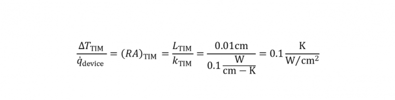
To quantify how this affects thermal resistance, we will look at the thermal resistance of a TIM per unit area, which can be quantified based on its thermal conductivity and thickness. Assuming perfect coverage and negligible contact resistance, a TIM with thickness of 0.1mm and thermal conductivity of 0.1W/cm-K results in:
To visualize the effect of the TIM at varying power levels, we can plot the temperature drop across the TIM as a function of device power density:
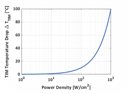
As shown in the semi log plot, for low power densities ~10W/cm^2, the effect of the TIM is negligible with only a ~1°C drop across the interface. However, in the case of a higher power density device, say around 500W/cm^2, the TIM can eat up over 50°C. Such a large drop across the TIM layer makes it very difficult to keep devices under their maximum allowable temperatures!
While there continues to be extensive research into new TIM materials and methodologies, even the most advanced TIMs are becoming prohibitive in high power density applications due to their limited thermal conductivity. Therefore, a different paradigm may be required to effectively cool high power density devices.
As one possible option, the figure below displays an instantiation of JetCool technology, where an ultra-high heat transfer coefficient fluid flow impinges directly on the electronic device. In this stackup, no TIMs or heat spreaders separate the fluid from the device, removing multiple layers of thermal resistance from the standard thermal stackup. This can be done at various stages of integration- whether at the package level as shown, or even down to the die level to bring the cooling as local to the heat generation as possible.

By bringing the fluid directly to the device surface, the thermal resistance of the TIM is removed, and the full device-fluid temperature difference can be utilized to remove heat. With typical device-fluid temperature differences between 25-150°C, heat transfer enhancements over 50% are not uncommon for power densities >500W/cm2 by obviating the TIM.
In summary, while TIMs offer a great solution to minimize contact resistance for many moderately powered devices, they are reaching their limits with an emerging class of electronics with high power density. Short of developments in TIMs that increase thermal conductivity by an order of magnitude or more, the newest class of high power density devices will benefit from new thermal architectures that bypass the TIMs and bring fluid directly to device surfaces.
Discover how liquid cooling can prepare your data center for sustainable AI computing in our latest data center, high-performance computing, and colocation case studies.


1 Comment