


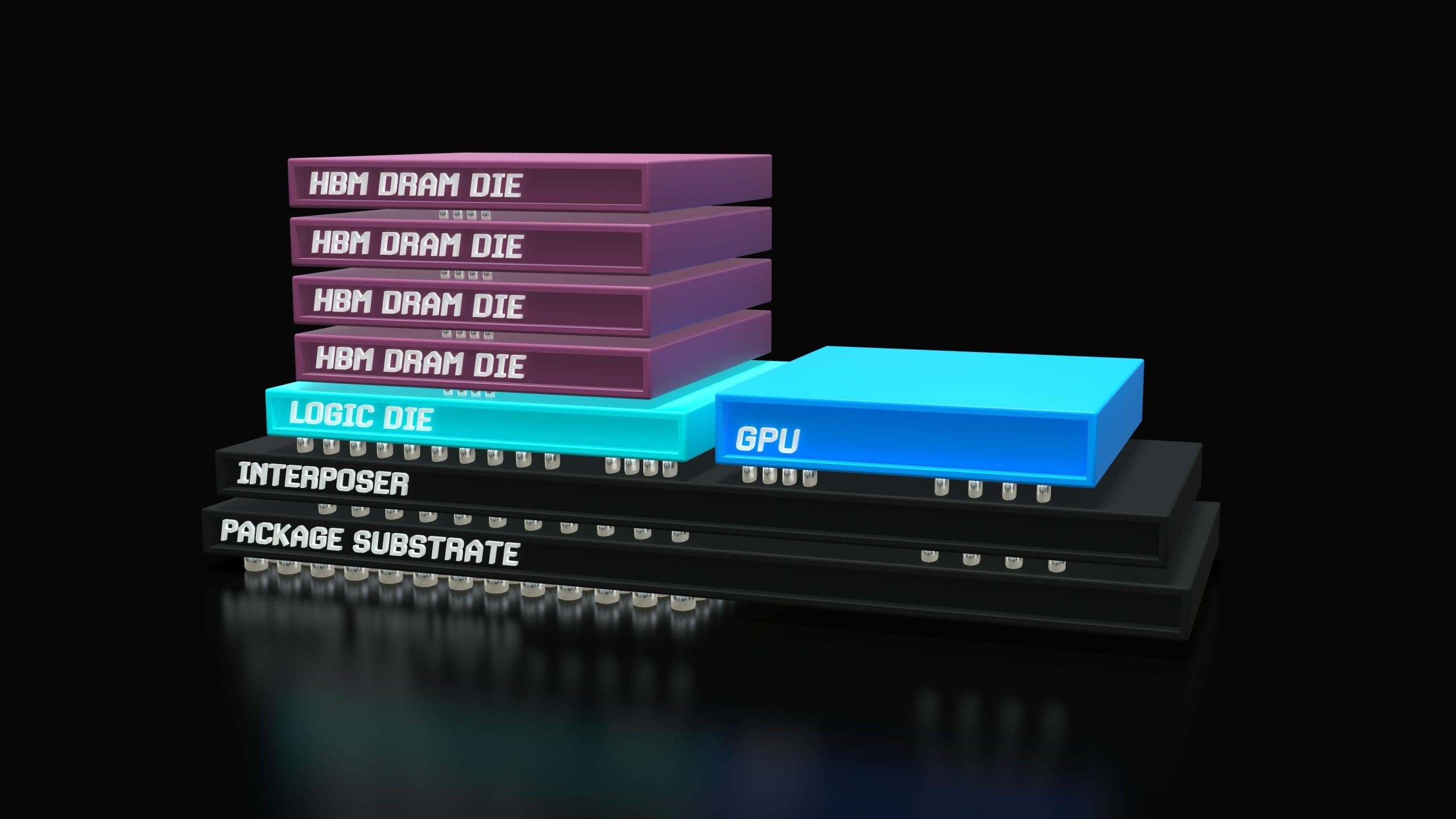
AI processors are only as effective as the data they can access. Today’s accelerators process data faster than conventional memory architectures deliver it, making memory bandwidth a critical constraint in next-generation chip design. High Bandwidth Memory (HBM) addresses that problem by moving memory into the processor package, increasing data transfer speeds, reducing bottlenecks, and supplying compute resources more efficiently. But that same architectural shift also changes the dynamics of processor cooling. By placing memory closer to the highest heat-generating components, HBM creates multiple thermal zones with distinct heat profiles, temperature limits, and cooling requirements within the processor package. That complexity starts at the silicon level, but it ripples outward through the server, rack, and data center facility.
In this blog, we’ll look at three reasons HBM is becoming the next AI cooling challenge: it places memory next to compute, accelerates the shift toward more complex processor packaging, and extends thermal design considerations beyond the chip.
Reason #1: Memory Is Now Co-Located with Compute
The conventional DRAM architecture where memory sits on separate modules and data travels across the board via electrical traces and interfaces, was not designed for that level of parallel demand. HBM solves this by vertically stacking multiple memory dies and placing them next to the processor on a shared interposer. By shortening the path between memory and compute, HBM delivers the bandwidth and speed required for AI training, inference, and high-performance computing. The result is an increasingly dense package in which memory and compute are integrated much more tightly.
The rapid adoption of AI marked a pivotal inflection point for HBM, accelerating its integration into mainstream data center architectures. Initially, HBM was used primarily in top-tier GPUs and accelerators for AI training and supercomputing. Now, it’s becoming a core element of AI processor roadmaps rather than a premium feature reserved for the most advanced systems. That shift is already visible across the processor ecosystem, including NVIDIA Hopper and Blackwell platforms, AMD Instinct MI300-class accelerators, Google TPU generations, and a growing number of hyperscale custom ASICs.


As HBM becomes foundational to AI processor design, it also changes a basic cooling assumption: memory is no longer physically separated from the hottest parts of the system. It is now co-located with compute inside the same processor package
That creates a direct thermal challenge. The compute die generates the highest heat flux, with hot spots that shift dynamically as workloads change. HBM stacks typically generate less heat than the processor core, but they are highly temperature sensitive. In an HBM-enabled package, the cooling system must manage both processor hot spots and the more stringent temperature requirements of nearby memory stacks. This makes precision-engineered thermal management a fundamental requirement for next-generation AI processors.
Reason #2: HBM Accelerates the Trend Toward More Complex Processor Packaging
In effect, the processor package is beginning to behave less like a single chip and more like a compact system of compute, memory, interconnect, and specialized logic. These designs can deliver major gains in bandwidth, latency, and performance per watt, but they also create more localized hot spots, more varied thermal requirements, and less uniform heat distribution across the package.
That is why HBM matters beyond its own thermal requirements. It provides an early look at where processor design is heading. As more functions are stacked, integrated, and placed closer together, cooling systems will need to be designed around the thermal profile of the full package rather than a single dominant heat source. HBM is one of the first visible examples of that future cooling challenge.
Reason #3: HBM Extends Thermal Design Beyond the Chip
Data center teams need to evaluate the full path around the cold plate: server layout, connector placement, rack manifolds, coolant distribution, CDU capacity, available flow, water temperature limits, pressure drop, redundancy, monitoring, service access, and facility water systems. If those requirements are addressed only after the servers arrive, deployment can be limited by the rack, CDU, or facility water loop rather than by the silicon or cold plate’s capability. Successful HBM cooling depends on matching a package-level thermal solution with the rack-level and facility-level infrastructure required to sustain it.
This is also why cooling considerations need to be accounted in package design, not addressed only after the chip and server architecture are already defined. As processor packages become denser and more thermally diverse, cooling cannot be treated as an afterthought. Semiconductor companies, OEMs, system designers, and cooling providers need to work together early so the chip package, server, rack, and facility can scale as one system.